The STEM platform in LPS hosts two cutting-edge scanning transmission electron microscopes (STEM), USTEM200 and CHROMATEM, providing support to a wide range of research fields in materials science, condensed matter physics, bio-imaging and nano-optics. We have special expertise in studying a variety of materials, including functional oxide materials, nuclear materials, semiconductors, plasmonic materials, 2D materials, catalytic nanoparticles or bio-materials among others. The main capabilities of the platform include:
- Direct sub-Å resolution imaging.
- 3 main operating voltages (60keV, 100keV, and 200keV)
- High energy resolution Electron Energy-Loss Spectroscopy (EELS) for the atomic-resolved chemical and bonding analysis
- Ultra-high resolution EELS for optical and vibrational analyses
- High spatial resolution cathodoluminescence (CL) spectroscopy for nano-optics studies.
- Liquid nitrogen temperature sample holders for fragile/beam sensitive samples
- Liquid nitrogen temperature sample holders coupled with MEMS for variable temperature and/or biasing in situ experiments.
- 4D STEM for complete structural information on crystal structure/orientation, strain distribution, electric field mapping.
- Smart scanning technologies including random scan for beam sensitive samples.
Platform manager:
Xiaoyan LI
xiaoyan.li@universite-paris-saclay.fr
Access to platform is free of charge and open to worldwide research community.
- French and international academic and industrial researchers can apply for the instrument/data analysis time through French microscope network METSA.
The plateform is also open with charges to special demands of industrial partners. Please contact our platform manager [xiaoyan.li@universite-paris-scalay.fr] for further information.
METSA:
METSA is a French research federation made up of 8 platforms, bring together a set of state-of-art expertise and equipment: 3 APT, 13 TEM including 6 Cs-corrected ones, and 3FIB. Two calls for projects are published each year (end of October and end of May). The projects are appraised by a set of specialists and a decision is notified to applicants within 6 weeks of filing. If successful, the requested experience is fully funded, and all or part of the applicant’s mission expenses are reimbursed. If you want to apply through METSA, it is highly recommended that you contact us to prepare the application.
TEMPOS:
TEMPOS, an “EquipEx” project funded by the French Governement “Investissement d’Avenir” program, stands for Transmission Electron Microscopy at Palaiseau, Orsay and Saclay: it unites the efforts of the Université Paris-Saclay (UPSaclay), Ecole polytechnique, CNRS, and CEA to create a world-class centre for transmission electron microscopy (TEM) in the Paris-Saclay area. TEMPOS is a three-pronged project, with two pieces of next-generation equipment devoted to excellence in TEM (CHROMATEM is one of these), and a third pole to back up the development of other local nanoscience activities. TEMPOS aims at expanding the frontiers in the study of individual nano-objects and nanomaterials, from their growth to the most local measurement of their physical properties, with innovative instrumentation. It also aims at providing support to the whole nanoscience community on the Campus and also enables the necessary preliminary studies required by the other two microscopes. Knowledge and technology transfer is eased by the presence of private companies (Thales RT, St Gobain Recherche) and joint venture laboratories (Thales-CNRS UMφ, St Gobain-CNRS SVI) in the consortium.
NION USTEM 200
- 60-200 kV cold FEG with ultra-high vacuum column
- C5 Nion QO corrector, with high spatial resolution (0.68 Å at 200 kV)
- EELS energy resolution is 0.27eV at 60kV.
- MerlinEM direct electron detector from Quantum detectors for EELS and 4D STEM.
- Double-tilt holder with a large tilt angle up to +/- 30 degree
- Ultrastable x, y, z sample stage with multi-holder in-vacuum magazine for convenient loading
- In situ holder with MEMS for heating (from 300 K to 1000 K) and electrical biasing from Protochips.
- Smart scanning technologies including random scan, live realignment and live spectral imaging at atom scales.
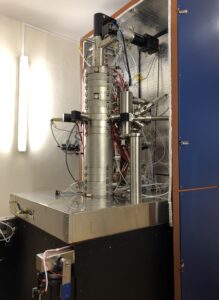
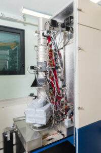
CHROMATEM
CHROMATEM is a monochromated and Cs-corrected scanning transmission electron microscope designed and built by NION based on the HERMES model, and adapted to some Orsay STEM team specifications, making it a world-wide unique machine for electron and photon spectromicroscopy.
Cyrill Fresillon LPS/CNRS images
- 30-200 kV cold FEG with ultra-high vacuum column
- Ultra- high energy resolution monochromator for sub-10 meV energy resolution (4.8meV at 30kV)
- Nion C5 QO aberration corrector for sub-Å spatial resolution (0.8 Å at 200kV)
- Swappable lastest direct electron detectors for EELS and 4D STEM:
- MerlinEM direct electron detector from Amsterdam Scientific Instruments(ASI).
- Event-based Cheetah Timepix from Amsterdam Scientific Instruments(ASI).
- Attolight Mönch cathodoluminescence detector with ultra-high sensibility and speed.
- Double/single tilt holder with a large tilt angle up to +/- 90 degree (alpha) and +/- 45 degree (beta).
- Liquid nitrogen temperature single-tilt holder from HennyZ, coupled with MEMS electrical biasing and highly accurate temperature control (125K-800K) options and high sample stability, compatible with cathodoluminescence system.
- Liquid nitrogen double-tilt temperature holder from HennyZ (α +/- 25 degree; β +/- 20 degree), equipped with MEMS electrical biasing and highly accurate temperature (125K-800K) control and high sample stability.
- Smart scanning technologies including random scan, live realignment and live spectral imaging at atom scale.
| Name of microscope | USTEM200 | CHROMATEM |
| Year of installation | 2011 | 2018 |
| Accelerating Voltage | 60 kV 100 kV 200 kV | 30 kV 60kV 100kV 200kV |
| Gun type | Cold FEG | Cold FEG |
| Excitation source | Electron | Electron Laser |
| Imaging techniques | HAADF MAADF ABF BF 4D STEM | HAADF MAADF ABF BF 4D STEM |
| Imaging resolution | 0.68 Å at 200kV 0.75 Å at 100kV 1 Å at 60kV | 0.8 Å at 200kV 1.2 Å at 100kV 2 Å at 60kV 3 Å at 30kV |
| Spectrometer | EELS-Merlin direct detector | EELS-Merlin direct detector Cathodoluminescence-Attolight |
| EELS energy resolution | 0.27 eV at 60kV | 15 meV at 200kV 10 meV at 100kV 7 meV at 60kV 4.8 meV at 30kV |
| In-situ options | Heating from 300K up to 1000K 2-points electrical biasing | Single and double-tilt Cooling/heating (125K to 800K) 2-points electrical biasing |