Paris-Saclay University
Biography
My research focuses on tuning the electronic properties through structural modifications. Objects of predilection are surfaces and other two-dimensional systems where physical properties can be significantly affected by quantum confinement in nanostructures, defects or phase transitions.
Interests
- Quantum confinement in nanostructures
- Phase transitions in low dimensional systems
- Spin-orbit coupling at surfaces and 2D materials
Education
- PhD in Condensed Matter, 2003 Université Autonome de Madrid, Espagne
- Accreditation to direct research (HDR), 2011 Université de Lorraine, France
Photoemission in solids : concepts and applications
Photoemission is a spectroscopic technique that allows to study the physicochemical properties of surfaces as well as their electronic properties, as it measures the band structure of materials.
This book introduces the main concepts of the photoemission technique : core level photoemission and valence band photoemission. It also presents a variety of recent developments on nowadays subjects. Two readings are possible. There is an elementary level based on a one-electron approach to understand qualitatively the interest of this spectroscopy. There is also a deeper level based on a many-electron approach allowing to study interactions in condensed matter physics.
This book has been conceived for a broad audience, from undergraduate students for the more elementary aspects to specialized researchers on the technique in the presentation of concepts and application examples.
Ballistic transport in graphene nanoribbons
Extreme miniaturization of electronic devices is closely related to heat dissipation problems. Heat dissipation can be significantly reduced by changing from silicon to carbon electronics, as it was known from the studies on carbon nanotubes that showed ballistic (i.e. lossless) transport there. Devices on carbon nanotubes are feasible although it is difficult to place nanotubes at will. Graphene is an easily patternable material, but the ballistic transport had to be demonstrated, because most of the graphene ribbons exhibited a transport gap, incompatible with ballistic transport. Sidewall graphene nanoribbons do not have a transport gap and have the ideal electronic structure of undoped graphene as we observed by tunnel spectroscopy and photoemission. Transport measurements demonstrate an exceptional ballistic transport up to 16 μm even at room temperature, making them promising for extreme device integration and for lossless interconnects.
On the left, electronic structure on the graphene ribbon obtained by photoemission. Right, transport measurements as a function of probe spacing for different annealing temperatures of the ribbons. All curves converge at h/e2. Figures from J. Baringhaus et al., Nature 506, 349 (2014).
Exceptional ballistic transport in epitaxial graphene nanoribbons. J. Baringhaus, M. Ruan, F. Edler, A. Tejeda, M. Sicot, A. Taleb Ibrahimi, Z. Jiang, E. Conrad, C. Berger, C. Tegenkamp, W. A. de Heer. Nature 506, 349 (2014).
Commented in Nature Physics News & Views 10, 182 (2014).
CNRS press release : http://www2.cnrs.fr/presse/communique/3419.htm.
Cover page of the CNRS annual report 2013.
Metal-insulator transition in Sn/Ge(111)
Upon deposition of 1/3 of atomic monolayer of Sn on Ge(111), a metallic reconstruction at room temperature. This reconstruction is sensitive to strong correlation effects, as its bands are rather narrow. The electrons at a same atom can no longer be considered as independent because of the electronic repulsion between electric charges of the same sign. The motion of electrons will be difficult due to this repulsion. The usual picture for describing the electronic properties of many materials (the band theory) is no longer valid. The band theory predicts these materials as metallic, while they are found to be insulating : they are called Mott insulators. We have identified experimental observations compatible with a Mott transition from a metallic to an insulating phase on Sn/Ge(111) below 30 K.
Observation of a Mott insulating ground state for Sn/Ge(111) at low temperature R. Cortés, A. Tejeda, J. Lobo, C. Didiot, B. Kierren, D. Malterre, E.G. Michel, et A. Mascaraque. Physical Review Letters 96, 126103 (2006).
http://dx.doi.org/10.1103/PhysRevLett.96.126103
Commented in Nature News & Views 441, 295 (2006).
Observation of the ideal dispersion on graphene
Graphene growing on the carbon face of SiC has a growth rate for a given temperature very different from that of Si face. Graphene layers on the C-face are stacked with angles different from 60°, the characteristic angle of graphite and of the Si-face. As the stacking is different from that of graphite, the electronic properties of ideal graphene are preserved, as proved by our photoemission measurements. Bands are linear for the different stacked layers and the doping of each layer is almost zero, as the Dirac point is located at the Fermi level.
Left figure from M. Sprinkle et al., Phys. Rev. Lett. 103, 226803 (2009). Copyright 2009 by the American Physical Society.” http://dx.doi.org/10.1103/PhysRevLett.103.226803
Band gap opening in graphene nanoribbons
We have studied the last-layer topography and beyond by combining scanning tunneling microscopy and transmission electron microscopy. The main body of the ribbons is bordered by regions where the SiC substrate has nanofacets. It is possible to grow a single graphene layer over the nanofacets as well as over the main facet. We have observed by photoemission that the electronic properties of the continuous graphene layer change depending on the region. On top of the nanofacets there are graphene nanoribbons. These nanoribbons are attached to the SiC substrate on their two edges, in a semiconducting region. The graphene between the attached parts is decoupled from the substrate and it exhibits a band gap of more than 500 meV because of the electronic confinement in these small nanoribbons of 1-2 nm width.
Schematics and details of the structure adapted with permission from I. Palacio et al., Nano Lett. 15, 182 (2015). Copyright 2015 American Chemical Society. Photoemission data from J. Hicks et al., Nature Phys 9, 49 (2012).
Electronic confinement in self-organized surfaces
The growth of self-organized systems can be used to tailor the electronic properties of the substrate. This is possible because surface states are localized in the last atomic layers and are sensitive to modifications in these layers. It is possible to create a self-organized network of islands that induces a periodic modification of the surface potential. In this way, a network of periodic quantum boxes can be settled to study their electronic properties. Co islands can be indeed self-organized on top of a stepped (vicinal) Au surface. The Au surface state is confined by the Co islands and the surface steps. The periodicity of the system allows to use photoemission to measure the band structure and obtain the surface potential.
On the left, differential conductance image of self-organized Co islands on a stepped substrate of Au. The intensity in between each four islands shows that the surface state is confined there. On the right, simulation of the photoemission measurements in order to determine the surface potential induced by Co islands.
“Interacting quantum box superlattice by self-organized Co nanodots on Au(788)”. C. Didiot, A. Tejeda, Y. Fagot-Revurat, V. Repain, B. Kierren, S. Rousset, and D. Malterre, Phys. Rev. B 76, 081404(R) (2007).
Metal-insulator transition and charge order in Sn/Ge(111)
The search for two dimensional Mott insulators has begun on the 1990s with K/Si(111):B and SiC(0001). In 2006, we have discovered a new metal-insulator transition for 1/3 ML Sn on Ge(111) under 30 K. We have interpreted these observations in terms of a Mott transition.
In Sn/Ge(111), the metallic (3×3) reconstruction that appears around 200 K was considered as the fundamental state. However, our complementary experiments of low energy electron diffraction, angle-resolved photoemission and scanning tunneling microscopy have allowed us to discover two new phases. Below 60 K the system becomes a bad metal while preserving the (3×3) surface symmetry. It is a charge ordered insulating phase. Under 30 K, the surface symmetry changes to (√3 x √3)R30°, where the vertical distortion of Sn atoms in the (3×3) phase is lost. All the Sn atoms are equivalent. Photoemission using synchrotron radiation shows that the structural phase transition, also observed in the core levels, is concomitant to a band gap opening. This experimental observations are compatible with the onset of a Mott insulating phase.
Phase transitions in Sn/Ge(111). Left column, Sn 4d core levels for three temperatures characteristic of each phase. Middle column, STM images showing the charge order in the intermediate phase and the equivalence of all the Sn atoms at the low temperature phase. Right column, electronic structure showing the bad metallicity of the intermediate phase and the large gap at the low temperature phase. Figures from R. Cortés et al., Phys. Rev. B 88, 125113 (2013). Copyright 2013 by the American Physical Society.” http://dx.doi.org/10.1103/PhysRevB.88.125113
D’autres références :
Observation of a Mott insulating ground state for Sn/Ge(111) at low temperature R. Cortés, A. Tejeda, J. Lobo, C. Didiot, B. Kierren, D. Malterre, E.G. Michel and A. Mascaraque. Physical Review Letters 96, 126103 (2006).
http://dx.doi.org/10.1103/PhysRevLett.96.126103
Highlight in Nature News & Views 441, 295 (2006).
Transition in Sn/Si(111):B by ultrafast collective diffusion
The Sn/Si(111) interface doped with B is a good candidate to look for Mott insulators, as it is hybrid between Sn/Si(111) and K/Si:B interfaces, both prone to exhibit electronic correlation effects. On Sn/Si(111):B we have found an insulating phase at room temperature that exhibits a reversible phase transition at 520 K, giving rise to a different surface symmetry. This phase transition is explained by a the collective fluctuation of Sn surface atoms at the picosecond scale. These fluctuations correspond to Sn tetramers exploring the 24 energy-degenerated configurations as a function of time.
Phase transition in Sn/Si(111):B. On the top, STM image showing the order of the Sn/Si(111):B surface at room temperature. On the bottow, low energy electron diffraction patterns showing the reversible symmetry change at the surface around 520 K. Figure from W. Srour et al., Phys. Rev. Lett. 114, 196101 (2015). Copyright 2015 by the American Physical Society.” http://dx.doi.org/10.1103/PhysRevLett.114.196101
Collective diffusion of Sn atoms. Atomic positions of surface atoms calculated by ab-initio molecular dynamics. Film from W. Srour et al., Phys. Rev. Lett. 114, 196101 (2015). Copyright 2015 by the American Physical Society.” http://dx.doi.org/10.1103/PhysRevLett.114.196101
Inverse photoemission
Inverse photoemission technique consists of illuminating a sample with low-energy electrons to proof the empty states of the materials. When electrons reach an empty state connected by an allowed transition to a lower energy empty state, the electron relaxation emits a photon providing information on the electronic transition. If both the kinetic energy of the electron beam and its incidence angle on the sample are known, it is possible to determine de empty state of the material. Angle resolved inverse photoemission (ARIPES) allows therefore to determine the conduction band of the studied system. If the electron beam has a well-defined spin orientation, the spin-resolved conduction band can be determined.
Principle of angle-resolved inverse photoemission. When electrons reach the sample and relax inside the solid, photons are emitted to preserve the energy conservation. If electrons reach the sample with a well-defined angle, the energy and momentum conservation at the surface allow to determine the empty states of the solid.
Direct photoemission
The photoemission technique is based on the photoelectric effect, explained by Albert Einstein in 1905, who was awarded the Nobel prize in 1921 because of its explanation. This phenomenon consists of the extraction of electrons in an illuminated material when the radiation is energetic enough. If both the kinetic energy and the emission angle of the emitted electron are detected, it is possible to determine de initial state at the material. Angle resolved photoemission (ARPES) allows therefore to determine the band structure of the studied system or the chemical composition by analysis of the core levels in the material.
Radiation sources to illuminate the sample can either be ultraviolet lamps, lasers, cathode-ray tubes or even synchrotrons like SOLEIL. In the synchrotrons, charged particles are stored in rings to use their wide spectra of emitted wavelengths.
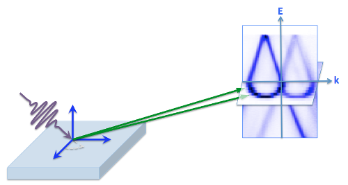
Principle of angle-resolved photoemission. When photons illuminate a sample, electrons are emitted by photoelectric effect. The energy and momentum conservation at the surface allow to determine the initial state of the electron in the solid.
Film on photoemission principle. Courtesy of Julien Bobroff.
Scanning tunneling microscopy
Scanning tunneling microscopy is a technique able to explore the electronic states at surfaces, reaching in this way to some topographic information. The Nobel prize was awarded to Gerd Karl Binnig and Heinrich Rohrer in 1986 for the first realisation of this instrument, which was shared with Ernst Ruska for the electronic microscope. The technique consists of approaching a tip to the sample. A voltage bias is settled between tip and surface. If the tip is close enough to the surface but there is no contact, electrons can flow between tip and sample due to the electrons that travel through the potential barrier by quantum tunneling. Topographic images can be obtained by scanning the surface with the tip. It is possible to constrain the tip-sample current to be constant during this process. In this way, the vertical tip displacement reports on the topography of the surface.
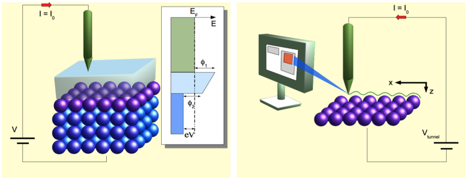
Scanning tunneling microscopy principle. A tip scans the sample and a voltage is settled between sample and tip. If the distance between them is small enough without contact, electrons can flow through the potential barrier between sample and tip by quantum tunneling. By recording the tip height variation when scanning the surface in a rectangular region, the STM image is obtained.
Film of the scanning tunneling microscopy principle. Courtoisy of Julien Bobroff.
X-ray diffraction
X-ray diffraction is a technique based on the interaction between X-rays and matter. William Lawrence Bragg and his father William Henri Bragg were awarded the Nobel prize in 1915 because of their development.
Diffraction results from the interference between X-rays that illuminate a material whose atoms are periodically disposed. X-rays are reflected on the different crystallographic planes of the material. There is a difference in the path of X-rays reflected in the different crystallographic planes of the material. The path difference is at the origin of interference phenomena between the different reflected beams, giving rise to maxima and minima of intensity. The angle where the maxima appear as well as their intensity contain structural information on the material. The analysis of these quantities allows to obtain a valuable information : the atomic positions.
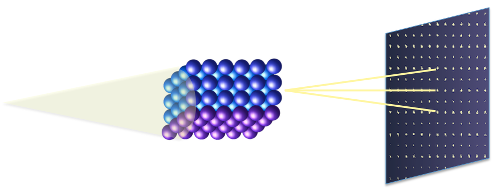
X-ray diffraction principle. X-ray interacting with a periodic system give rise to an intensity redistribution after interaction. The analysis of this intensity as well as its angular distribution allows to determine the atomic structure of the material.
Film on crystallography and reciprocal space. Courtoisy of Julien Bobroff.
Spin- and angle-resolved inverse photoemission setup with spin orientation independent from electron incidence angle., A. F. Campos, P. Duret, S. Cabaret, T. Duden, A. Tejeda Review of Scientific Instruments 93, 093904 (9p) (2022).
CNRS press release: https://www.inp.cnrs.fr/fr/cnrsinfo/le-spin-dans-toutes-ses-orientations
Renormalization of the valence and conduction bands of (C6H5C2H4NH3)2PbI4 hybrid perovskite. Min-I Lee, S. Ayaz Khan, H. Mrezguia, A. Barragan, M. N. Nair, H. Khelidj, Y. Ksari, L. Giovanelli, J.-M. Themlin, F. Lédée, G. Trippé-Allard, E. Deleporte, A. Taleb-Ibrahimi, J. Minar, Antonio Tejeda
Journal of Physics D: Applied Physics 54, 365301 (7p) (2021).
Edge states and ballistic transport in zigzag graphene ribbons: The role of SiC polytypes. A. L. Miettinen, M. S. Nevius, W. Ko, M. Kolmer, A. P. Li, M. N. Nair, B. Kierren, L. Moreau, E. H. Conrad, A. Tejeda,
Physical Review B 100, 045425 (8p) (2019).
Superlattice-induced minigaps in graphene band structure due to underlying one-dimensional nanostructuration. A. Celis, M. N. Nair, M. Sicot, F. Nicolas, S. Kubsky, D. Malterre, A. Taleb-Ibrahimi, A. Tejeda.
Physical Review B 97, 195410 (6p) (2018).
Time resolved photoemission spectroscopy of electronic cooling and localization in CH3NH3PbI3. Z. Chen, Min-i Lee, Z. Zhang, H. Diab, D. Garrot, F. Lédée, P. Fertey, E. Papalazarou, M. Marsi, C. Ponseca, E. Deleporte, A. Tejeda, L. Perfetti,
Physical Review Materials 1, 045402 (6p) (2017).
First determination of the valence band dispersion of CH3NH3PbI3 hybrid organic–inorganic perovskite. M.-I Lee, A. Barragán, M.N. Nair, V.L.R. Jacques, D. Le Bolloc’h, P. Fertey, K. Jemli, F. Lédée, G. Trippé-Allard, E. Deleporte, A. Taleb-Ibrahimi, A. Tejeda.
Journal of Physics D: Applied Physics 50, 26LT02 (10p) (2017).
Article invité.
Band gap opening induced by the structural periodicity on the graphene buffer layer. M.N. Nair, I. Palacio, A. Celis, A. Zobelli, A. Gloter, S. Kubsky, J.-P. Turmaud, M. Conrad, C. Berger, W.A. de Heer, E.H. Conrad, A. Taleb-Ibrahimi, A. Tejeda.
Nano Letters. 17, 2681 (9p) (2017).
Semiconducting Graphene from Highly Ordered Substrate Interactions.
M.S. Nevius, M. Conrad, F. Wang, A. Celis, M.N. Nair, A. Taleb-Ibrahimi, A. Tejeda, and E.H. Conrad,
Physical Review Letters 115, 136802 (2015).
Commenté dans Physics 8, 91 (2015).
Ultrafast atomic diffusion inducing a reversible (2√3 × 2√3)R30◦ ↔ (√3 × √3)R30° transition on Sn/Si(111):B.
W. Srour, D.G. Trabada, J. I. Martínez, F. Flores, J. Ortega, M. Abuín, Y. Fagot-Revurat, B. Kierren, P. Le Fèvre, A. Taleb-Ibrahimi, D. Malterre, A. Tejeda.
Physical Review Letters 114, 196101 (2015).
Atomic Structure of Epitaxial Graphene Sidewall Nanoribbons: Flat Graphene, Miniribbons, and the Confinement Gap.
I. Palacio, A. Celis, M. N. Nair, A. Gloter, A. Zobelli, M. Sicot, D. Malterre, M. S. Nevius, C. Berger, W. A. de Heer, E. H. Conrad, A. Taleb-Ibrahimi, A. Tejeda.
Nano Letters 15, 182 (2015).
Exceptional ballistic transport in epitaxial graphene nanoribbons.
J. Baringhaus, M. Ruan, F. Edler, A. Tejeda, M. Sicot, A. Taleb Ibrahimi, Z. Jiang, E. Conrad, C. Berger, C. Tegenkamp, W. A. de Heer.
Nature 506, 349 (2014).
Communiqué de presse CNRS: http://www2.cnrs.fr/presse/communique/3419.htm.
Page de garde du rapport d’activités du CNRS 2013.
Commenté dans Nature Physics News & Views 10, 182 (2014).
Hydrogen-induced nanotunnel opening within semiconductor sub-surface.
P. Soukiassian, E. Wimmer, E. Celasco, C. Giallombardo, S. Bonanni, L. Vattuone, L. Savio, A. Tejeda, M. Silly, M. D’angelo, F. Sirotti, M. Rocca.
Nature Communications 4, 2800 (2013).
A wide band gap metal-semiconductor-metal nanostructure made entirely from graphene.
J. Hicks, A. Tejeda, A. Taleb-Ibrahimi, M.S. Nevius, F. Wang, K. Shepperd, J. Palmer, F. Bertran, P. Le Fèvre, J. Kunc, W.A. de Heer, C. Berger, et E.H. Conrad.
Nature Physics 9, 49 (2012).
Communiqué de presse CNRS: http://www2.cnrs.fr/presse/communique/2875.htm.
First direct observation of a nearly ideal graphene band structure.
M. Sprinkle, D. Siegel Y. Hu, J. Hicks, A. Tejeda, A. Taleb-Ibrahimi, P. Le Fèvre, F. Bertran, S. Vizzini, H. Enriquez, S. Chiang, P. Soukiassian, C. Berger, W. A. de Heer, A. Lanzara, and E. H. Conrad.
Physical Review Letters 103, 226803 (2009).
Structural origin of the Sn 4d core level line shape in Sn/Ge(111)-(3×3).
A. Tejeda, R. Cortés, J. Lobo-Checa, C. Didiot, B. Kierren, , D. Malterre, E. G. Michel, A. Mascaraque.
Physical Review Letters 100, 026103 (2008).
Observation of a Mott insulating ground state for Sn/Ge(111) at low temperature. R. Cortés, A. Tejeda, J. Lobo, C. Didiot, B. Kierren, D. Malterre, E.G. Michel, et A. Mascaraque.
Physical Review Letters 96, 126103 (2006).
Page de garde de son numéro.
Commenté en Nature News & Views 441, 295 (2006).
Uniform Magnetic Properties for an Ultrahigh-Density Lattice of Noninteracting Co Nanostructures.
N. Weiss, T. Cren, M. Epple, S. Rusponi, G. Baudot, S. Rohart, A. Tejeda, V. Repain, S. Rousset, P. Ohresser, F. Scheurer, P. Bencok, H. Brune
Physical Review Letters 95, 157204 (2005).
*First determination of the valence band dispersion of CH3NH3PbI3 hybrid organic–inorganic perovskite. M.-I Lee, A. Barragán, M.N. Nair, V.L.R. Jacques, D. Le Bolloc’h, P. Fertey, K. Jemli, F. Lédée, G. Trippé-Allard, E. Deleporte, A. Taleb-Ibrahimi, A. Tejeda.
Journal of Physics D: Applied Physics 50, 26LT02 (10p) (2017).
* Graphene nanoribbons: fabrication, properties and devices.
A Celis, M N Nair, A Taleb-Ibrahimi, E H Conrad, C Berger, W A de Heer, A Tejeda.
Journal of Physics D: Applied Physics 49, 143001 (2016).
* Understanding the Insulating Ground State Properties of Alkali-Metal/Si(111):B Interfaces.
Y. Fagot-Revurat, C. Tournier-Colletta, L. Chaput, A. Tejeda, L. Cardenas, B. Kierren, D. Malterre, P. Le Fèvre, F. Bertran, A. Taleb-Ibrahimi.
Journal of Physics: Condensed Matter 25, 094004 (2013).
* Electron correlation and many-body effects at interfaces on semiconducting substrates.
A. Tejeda, Y. Fagot-Révurat, R. Cortés, D. Malterre, E. G. Michel, A. Mascaraque.
physica status solidi (a) 209, 614 (2012).
Page de garde arrière de son numéro.
* Electronic properties of epitaxial graphene grown on the C-face of SiC and their relation to the structure.
A. Tejeda, A. Taleb-Ibrahimi, C. Berger, E.H. Conrad, W. de Heer.
New Journal of Physics 14, 125007 (2012).
* ARPES and STS investigation of Shockley States in thin metallic films and periodic nanostructures.
D. Malterre, B. Kierren, Y. Fagot-Revurat, S. Pons, A. Tejeda, C. Didiot, H. Cercellier, A. Bendounan.
New Journal of Physics 9, 391 (2007).
* The Fermi surface of Sn and Pb on Ge(111).
A. Tejeda, R. Cortés, J. Lobo, E.G. Michel, A. Mascaraque.
Journal of Physics : Condensed Matter 19, 355008 (2007).
* The photoelectron diffraction technique applied to advanced materials.
A. Tejeda et E.G. Michel.
Journal of Physics: Condensed Matter 16, 3441 (2004).
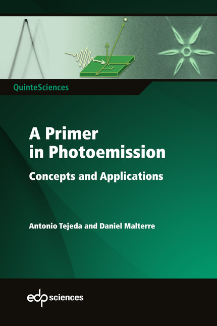
A primer in photoemission: concepts and applications,
A. Tejeda and D. Malterre,
EDP Sciences, Les Ulis 2019
Graphene nanoribbons : fundamentals, fabrication and devices,
edited by L.Brey, P.Seneor and A.Tejeda
IOP, Bristol 2020.
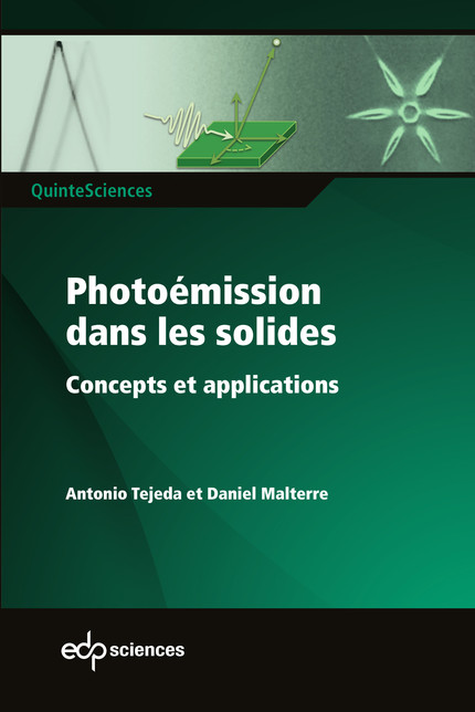
Photoémission dans les solides : concepts et applications,
A. Tejeda and D. Malterre,
EDP Sciences, Les Ulis 2015
- Min-I LEE (2015-2018) Atomic structure, electronic states and relaxation dynamics in photovoltaic materials and interfaces from photoemission-related spectroscopies.
- Arlensiú CELIS (2013-2016) Gap of graphene on nanostructured surfaces of SiC and on vicinal surfaces of noble metals.
- Waked SROUR (2009-2012) Propriétés structurales et électroniques de Sn/Ge/Si(111), Sn/Si(111):B et analogie entre intensités photoémise et diffractée en surface superpériodiques”.
Les propriétés du graphène sur un millefeuille.
A. Tejeda, A. Taleb-Ibrahimi et C. Berger.
Reflets de la physique 34-35, 84 (2013).
Les isolants de Mott, des conducteurs bloqués.
A. Tejeda et A. Mascaraque.
Pour la science (février 2012).
Isolant ou métal ?.
A. Tejeda et A. Mascaraque.
Investigacion y Ciencia (mars 2011).
83. Spin- and angle-resolved inverse photoemission setup with spin orientation independent from electron incidence angle., A. F. Campos, P. Duret, S. Cabaret, T. Duden, and A. Tejeda (submitted to Review of Scientific Instruments).
82. Photoemission image of momentum dependent hybridization in CeCoIn5. R. Kurleto, M. Fidrysiak, L. Nicolaï, J. Minár, M. Rosmusa, L. Walczak, A. Tejeda, J.E. Rault, F. Bertran, A.P. Kadzielawa, D. Legut, D. Gnida, D. Kaczorowski, K. Kissner, F. Reinert, J. Spałek, P. Starowicz, Physical Review B 104, 125104 (14p) (2021).
81. Substrate effect on the electronic properties of graphene on vicinal Pt(111). M. N. Nair, A. Celis, F. Nicolas, S. Kubsky, A. Taleb-Ibrahimi, A. Tejeda. Applied Surface Science 565, 150593 (7p) (2021).
80. Renormalization of the valence and conduction bands of (C6H5C2H4NH3)2PbI4 hybrid perovskite. Min-I Lee, S. Ayaz Khan, H. Mrezguia, A. Barragan, M. N. Nair, H. Khelidj, Y. Ksari, L. Giovanelli, J.-M. Themlin, F. Lédée, G. Trippé-Allard, E. Deleporte, A. Taleb-Ibrahimi, J. Minar, Antonio Tejeda Journal of Physics D: Applied Physics 54, 365301 (7p) (2021).
79. Doping Graphene with Substitutional Mn, P.-C. Lin, R. Villarreal, S. Achilli, H. Bana, M. N. Nair, A. Tejeda, K. Verguts, S. De Gendt, M. Auge, H. Hofsass, S. De Feyter, G. Di Santo, L. Petaccia, S. Brems, G. Fratesi, L. M. C. Pereira, ACS Nano 15, 5449 (10p) (2021)
78. Growth, morphology and electronic properties of epitaxial graphene on vicinal Ir(332) surface. A Celis, M.N. Nair, M Sicot, F Nicolas, S Kubsky, A Taleb-Ibrahimi, D Malterre, A Tejeda. Nanotechnology 31, 285601 (8p) (2020).
77. Hybrid Perovskites for Photovoltaics and Optoelectronics. A. Tejeda, W.C.H. Choy, E. Deleporte, M. Grätzel. Journal of Physics D: Applied Physics 53, 070201 (2p) (2020).
Préface pour le numéro spécial “Hybrid Perovskites for Photovoltaics and Optoelectronics ”.
76. Edge states and ballistic transport in zigzag graphene ribbons: The role of SiC polytypes. A. L. Miettinen, M. S. Nevius, W. Ko, M. Kolmer, A. P. Li, M. N. Nair, B. Kierren, L. Moreau, E. H. Conrad, A. Tejeda, Physical Review B 100, 045425 (8p) (2019).
75. A new long-range sub-structure found in the tetragonal phase of CH3NH3PbI3 single crystals. V.L.R. Jacques, A. Frantz-Gallo, A.Tejeda, D. Le Bolloc’h, F. Lédée, G. Trippé-Allard, D. Garrot, P. Fertey, E. Deleporte, O. Plantevin. Journal of Physics D: Applied Physics (10p) 52, 314001 (2019).
74. Effective determination of surface potential landscapes from metal-organic nanoporous network overlayers. I. Piquero-Zulaica, Z. Abd El-Fattah, O. Popova, S. Kawai, S. Nowakowska, M. Matena, M. Enache, M. Stöhr, A. Tejeda, A. Taleb-Ibrahimi, E. Meyer, J. Ortega, L. Gade, T. Jung, J. Lobo-Checa. New Journal of Physics (9p) 21, 053004 (2019).
73. Defect State Analysis in Ion-Irradiated Amorphous-Silicon Heterojunctions by HAXPES. M-I Lee, A. Defresne, O. Plantevin, D. Ceolin, J.-P. Rueff, P. Roca i Cabarrocas, A. Tejeda. physica status solidi Rapid Research Letters 1800655 (5p) (2019).
72. Superlattice-induced minigaps in graphene band structure due to underlying one-dimensional nanostructuration. A. Celis, M. N. Nair, M. Sicot, F. Nicolas, S. Kubsky, D. Malterre, A. Taleb-Ibrahimi, A. Tejeda.
Physical Review B 97, 195410 (6p) (2018).
71. Time resolved photoemission spectroscopy of electronic cooling and localization in CH3NH3PbI3. Z. Chen, Min-i Lee, Z. Zhang, H. Diab, D. Garrot, F. Lédée, P. Fertey, E. Papalazarou, M. Marsi, C. Ponseca, E. Deleporte, A. Tejeda, L. Perfetti,
Physical Review Materials 1, 045402 (6p) (2017).
70. Do 2D materials stack in a van der Waals fashion?». A. Tejeda,
Journal of Physics D: Applied Physics 50, 351001 (2p) (2017).
Présentation de l’article Di Felice D et al. J. Phys. D: Appl. Phys. 50, 17LT02 (2017)
69. First determination of the valence band dispersion of CH3NH3PbI3 hybrid organic–inorganic perovskite. M.-I Lee, A. Barragán, M.N. Nair, V.L.R. Jacques, D. Le Bolloc’h, P. Fertey, K. Jemli, F. Lédée, G. Trippé-Allard, E. Deleporte, A. Taleb-Ibrahimi, A. Tejeda.
Journal of Physics D: Applied Physics 50, 26LT02 (10p) (2017).
Article invité.
68. Band gap opening induced by the structural periodicity on the graphene buffer layer. M.N. Nair, I. Palacio, A. Celis, A. Zobelli, A. Gloter, S. Kubsky, J.-P. Turmaud, M. Conrad, C. Berger, W.A. de Heer, E.H. Conrad, A. Taleb-Ibrahimi, A. Tejeda.
Nano Letters. 17, 2681 (9p) (2017).
67. Wide band gap semiconductor from a hidden 2D incommensurate graphene phase. M. Conrad, F. Wang, M.S. Nevius, K. Jinkins, A. Celis, M.N. Nair, A. Taleb-Ibrahimi, A. Tejeda, Y. Garreau, A. Vlad, A. Coati, P.F. Miceli, E.H. Conrad.
Nano Letters. 17, 341 (2017).
66. Narrow Linewidth Excitonic Emission in Organic–Inorganic Lead Iodide Perovskite Single Crystals. H. Diab, G. Trippé-Allard, F. Lédée, K. Jemli, C. Vilar, G. Bouchez, V.L.R. Jacques, A. Tejeda, J. Even, J.-S. Lauret, E. Deleporte, D. Garrot,
Journal of Physical Chemistry Letters 7, 5093 (2016).
65. Graphene nanoribbons: fabrication, properties and devices.
A. Celis, M. N. Nair, A. Taleb-Ibrahimi, E. H. Conrad, C. Berger, W. A. de Heer, A. Tejeda.
Journal of Physics D: Applied Physics 49, 143001 (2016).
Article invité.
64. Uncertainty principle for experimental measurements: Fast versus slow probes.
E. Wimmer, E. Celasco, L. Vattuone, L. Savio, A. Tejeda, M. Silly, M. D’angelo, F. Sirotti, M. Rocca, A. Catellani, G. Galli, L. Douillard, F. Semond, V.Yu. Aristov, P. Soukiassian.
Surface Science Letters 644, L170 (2016).
63. Comment on “Adsorption of hydrogen and hydrocarbon molecules on SiC(001)” by Pollmann et al. (Surf. Sci. Rep. 69 (2014) 55–104).
E. Wimmer, E. Celasco, L. Vattuone, L. Savio, A. Tejeda, M. Silly, M. D’angelo, F. Sirotti, M. Rocca, A. Catellani, G. Galli, L. Douillard, F. Semond, V.Yu. Aristov, P. Soukiassian.
Surface Science Letters 644, L170 (2016).
62. Semiconducting Graphene from Highly Ordered Substrate Interactions.
M.S. Nevius, M. Conrad, F. Wang, A. Celis, M.N. Nair, A. Taleb-Ibrahimi, A. Tejeda, and E.H. Conrad,
Physical Review Letters 115, 136802 (2015).
Commenté dans Physics 8, 91 (2015).
61. Charge transfer and electronic doping in nitrogen-doped graphene.
F. Joucken, Y. Tison, P. Le Fèvre, A. Tejeda, A. Taleb-Ibrahimi, E. Conrad, V. Repain, C. Chacon, A. Bellec, Y. Girard, S. Rousset, J. Ghijsen, R. Sporken, J. Lagoute.
Scientific Reports 5, 14564 (2015).
60. Fermi surface symmetry and evolution of the electronic structure across the paramagnetic-helimagnetic transition in MnSi/Si(111).
A. Nicolaou, M. Gatti, E. Magnano, P. Le Fèvre, F. Bondino, F. Bertrand, A. Tejeda, M. Sauvage-Simkin, A. Vlad, Y. Garreau, A. Coati, N. Guérin, F. Parmigiani, A. Taleb-Ibrahimi.
Physical Review B 92, 081110(R) (2015).
59. Ultrafast atomic diffusion inducing a reversible (2√3 × 2√3)R30◦ ↔ (√3 × √3)R30° transition on Sn/Si(111):B.
W. Srour, D.G. Trabada, J. I. Martínez, F. Flores, J. Ortega, M. Abuín, Y. Fagot-Revurat, B. Kierren, P. Le Fèvre, A. Taleb-Ibrahimi, D. Malterre, A. Tejeda.
Physical Review Letters 114, 196101 (2015).
58. Atomic Structure of Epitaxial Graphene Sidewall Nanoribbons: Flat Graphene, Miniribbons, and the Confinement Gap.
I. Palacio, A. Celis, M. N. Nair, A. Gloter, A. Zobelli, M. Sicot, D. Malterre, M. S. Nevius, C. Berger, W. A. de Heer, E. H. Conrad, A. Taleb-Ibrahimi, A. Tejeda.
Nano Letters 15, 182 (2015).
57. Atomic and electronic structure of the (2√3×2√3)R30° strained Sn reconstruction on Ge/Si(111).
W. Srour, A. Tejeda, M. Stoffel, M. Abuín, Y. Fagot-Revurat, P. Le Fèvre, A. Taleb-Ibrahimi, D. Malterre.
Journal of Electron Spectroscopy and Related Phenomena 195, 174 (2014).
56. Walking peptide on Au(110) surface: Origin and nature of interfacial process.
V. Humblot, A. Tejeda, J. Landoulsi, A. Vallée, A. Naitabdi, A. Taleb, C.M. Pradier.
Surface Science 628, 21 (2014).
55. Exceptional ballistic transport in epitaxial graphene nanoribbons.
J. Baringhaus, M. Ruan, F. Edler, A. Tejeda, M. Sicot, A. Taleb Ibrahimi, Z. Jiang, E. Conrad, C. Berger, C. Tegenkamp, W. A. de Heer.
Nature 506, 349 (2014).
Communiqué de presse CNRS: http://www2.cnrs.fr/presse/communique/3419.htm.
Page de garde du rapport d’activités du CNRS 2013.
Commenté dans Nature Physics News & Views 10, 182 (2014).
54. Graphene: from functionalization to devices.
A. Tejeda et P. Soukiassian.
Journal of Physics D: Applied Physics 47, 090201 (2014).
Préface pour le numéro spécial “Graphene : from funcionalization to devices”.
53. Hydrogen-induced nanotunnel opening within semiconductor sub-surface.
P. Soukiassian, E. Wimmer, E. Celasco, C. Giallombardo, S. Bonanni, L. Vattuone, L. Savio, A. Tejeda, M. Silly, M. D’angelo, F. Sirotti, M. Rocca.
Nature Communications 4, 2800 (2013).
52. Wide-gap Semiconducting Graphene from Nitrogen-seeded SiC.
F. Wang, G. Liu, S. Rothwell, M. Nevius, A. Tejeda, A. Taleb-Ibrahimi, L. Feldman, P. Cohen, E. Conrad.
Nano Letters 13, 4827 (2013).
51. Competing charge ordering and Mott phases in a correlated Sn/Ge(111) two-dimensional triangular lattice.
R. Cortés, A. Tejeda, J. Lobo-Checa, C. Didiot, B. Kierren, D. Malterre, J. Merino, F. Flores, E. G. Michel, A. Mascaraque.
Physical Review B 88, 125113 (2013).
50. The dimensionality reduction at surfaces as a playground for many-body and correlation effects.
A. Tejeda, E.G. Mascaraque, E.G. Michel.
Journal of Physics: Condensed Matter 25, 090301 (2013).
Préface pour la section spéciale “Correlation and many-body effects at surfaces”.
49. Understanding the Insulating Ground State Properties of Alkali-Metal/Si(111):B Interfaces.
Y. Fagot-Revurat, C. Tournier-Colletta, L. Chaput, A. Tejeda, L. Cardenas, B. Kierren, D. Malterre, P. Le Fèvre, F. Bertran, A. Taleb-Ibrahimi.
Journal of Physics: Condensed Matter 25, 094004 (2013).
Article invité.
48. The (2√3×2√3)R30˚ surface reconstruction of alkali/Si(111):B semiconducting surfaces.
C. Tournier-Colletta, L. Chaput, A. Tejeda, L.A. Cardenas, B. Kierren, D. Malterre, Y. Fagot-Révurat.
Applied Surface Science 267, 35 (2013).
47. A wide band gap metal-semiconductor-metal nanostructure made entirely from graphene.
J. Hicks, A. Tejeda, A. Taleb-Ibrahimi, M.S. Nevius, F. Wang, K. Shepperd, J. Palmer, F. Bertran, P. Le Fèvre, J. Kunc, W.A. de Heer, C. Berger, et E.H. Conrad.
Nature Physics 9, 49 (2012).
Communiqué de presse CNRS: http://www2.cnrs.fr/presse/communique/2875.htm.
46. Electron-phonon coupling on strained Ge/Si(111)-(5×5) surfaces.
M. Stoffel, Y. Fagot-Révurat, A. Tejeda, A. Nicolaou, B. Kierren, D. Malterre, P. Le Fèvre, F. Bertran, A. Taleb-Ibrahimi.
Physical Review B 86, 195438 (2012).
45. Surface electronic structure of InSb(001)-c(8×2).
L. Walczak, G. Goryl, M.A. Valbuena, I. Vobornik, A. Tejeda, A. Taleb-Ibrahimi, J.J. Kolodziej, M.A. Valbuena, P. Segovia, E.G. Michel.
Surface Science 608, 22 (2012).
44. Experimental correlation between photoemission matrix elements and LEED intensities in superperiodic structures.
W. Srour, A. Tejeda, A. Nicolaou, P. Le Fèvre, F. Bertran, A. Taleb-Ibrahimi, D. Malterre.
Journal of Electron Spectroscopy and Related Phenomena 185, 441 (2012).
43. Spin polarized electron tunneling in bcc FeCo/MgO/FeCo(001) magnetic tunnel junctions.
F. Bonell, T. Hauet, S. Andrieu, F. Bertran, P. Le Fèvre, L. Calmels, A. Tejeda, F. Montaigne, B. Warot-Fonrose, B. Belhadji, A. Nicolaou, A. Taleb-Ibrahimi,
Physical Review Letters 108, 176602 (2012).
42. Electron correlation and many-body effects at interfaces on semiconducting substrates.
A. Tejeda, Y. Fagot-Révurat, R. Cortés, D. Malterre, E. G. Michel, A. Mascaraque. physica status solidi (a) 209, 614 (2012).
Article invité. Page de garde arrière de son numéro.
41. High van Hove singularity extension and Fermi velocity increase in epitaxial graphene functionalized by intercalated gold clusters.
M. Nair, M. Cranney, F. Vonau, D. Aubel, P. Le Fèvre, A. Tejeda, F. Bertran, A. Taleb-Ibrahimi, L. Simon.
Physical Review B 85, 245421 (2012).
40. Silicon intercalation into the graphene-SiC interface.
F. Wang, K. Shepperd, J. Hicks, M. Nevius, H. Tinkey, A. Tejeda, A. Taleb-Ibrahimi, F. Bertran, P. Le Fèvre, D. Torrance, P. First, W. de Heer, A. Zakharov, E. Conrad.
Physical Review B 85, 165449 (2012).
39. Electronic properties of epitaxial graphene grown on the C-face of SiC and their relation to the structure.
A. Tejeda, A. Taleb-Ibrahimi, C. Berger, E.H. Conrad, W. de Heer.
New Journal of Physics 14, 125007 (2012).
Article invité.
38. Giant alkali-metal-induced lattice relaxation as the driving force of the insulating phase of alkali/Si(111):B.
L. Chaput, C. Tournier-Colletta, L.A. Cardenas, A. Tejeda, B. Kierren, D. Malterre, Y. Fagot-Révurat, P. Le Fèvre, F. Bertran, A. Taleb-Ibrahimi, D. González, J. Ortega, F. Flores.
Physical Review Letters 107, 187603 (2011).
37. Absolute coverage determination in the K/Si(111):B – (2√3×2√3)R30˚ surface.
C. Tournier-Colletta, L. Cardenas, Y. Fagot-Révurat , B. Kierren, A. Tejeda, D. Malterre.
Physical Review B 84, 155443 (2011).
36. Symmetry breaking in commensurate graphene rotational stacking: Comparison of theory and experiment.
J. Hicks, M. Sprinkle, K. Shepperd, F. Wang, A. Tejeda, A. Taleb-Ibrahimi, F. Bertran, P. Le Fèvre, W. A. de Heer, C. Berger, E. H. Conrad.
Physical Review B 83, 205403 (2011).
Editors’ suggestion.
35. Bipolaronic insulator on alkali/Si(111) – (2√3 × 2√3) R30˚ interfaces.
C. Tournier-Colletta, Cardenas, Y. Fagot-Revurat, B. Kierren, A. Tejeda, D. Malterre, P. Le Fèvre, F. Bertran, A. Taleb-Ibrahimi.
Physical Review B 82, 165429 (2010).
34. Structure of the indium-rich InSb(001) surface.
G. Goryl, D. Toton, N. Tomaszewska, J.S. Prauzner-Bechcicki L. Walczak, A. Tejeda, A. Taleb-Ibrahimi, L. Kantorovich, E.G. Michel, J.J. Kolodziej.
Physical Review B 82, 165311 (2010).
33. Multilayer epitaxial graphene grown on the SiC (000-1) surface; structure and electronic properties.
M. Sprinkle, J. Hicks, A. Tejeda, A. Taleb-Ibrahimi, P. Le Fèvre, F. Bertran, H. Tinkey, M.C. Clark, P. Soukiassian, D. Martinotti, J. Hass, E.H. Conrad.
Journal of Physics D 43, 374006 (2010).
32. New electronic orderings observed in cobaltates under the influence of misfit periodicities.
A. Nicolau, V. Brouet, M. Zacchigna, I. Vobornik, A. Tejeda, A. Taleb-Ibrahimi, P. Le Fèvre, F. Bertran, C. Chambon, S. Hébert, H. Muguerra, D. Grebille.
Europhysics Letters 89, 37010 (2010).
31. Experimental study of the incoherent spectral weight in the photoemission spectra of the misfit cobaltate [Bi2Ba2O4][CoO2]2.
A. Nicolaou, V. Brouet, M. Zacchigna, I. Vobornik, A. Tejeda, A. Taleb-Ibrahimi, P. Le Fèvre, F. Bertran, S. Hébert, H. Muguerra, D. Grebille.
Physical Review Letters 104, 056403 (2010).
30. First direct observation of a nearly ideal graphene band structure.
M. Sprinkle, D. Siegel Y. Hu, J. Hicks, A. Tejeda, A. Taleb-Ibrahimi, P. Le Fèvre, F. Bertran, S. Vizzini, H. Enriquez, S. Chiang, P. Soukiassian, C. Berger, W. A. de Heer, A. Lanzara, and E. H. Conrad.
Physical Review Letters 103, 226803 (2009).
29. Spin Reorientation Transition and Magnetic Domain Structure of the Co Ultra-thin Films Grown on Faceted Au(455) Surface.
J. Gao, Y. Girard, V. Repain, A. Tejeda, R. Belkhou, N. Rougemaille, C. Chacon, G. Rodary, S. Rousset.
Physical Review B 77, 134429 (2008).
28. Structural origin of the Sn 4d core level line shape in Sn/Ge(111)-(3×3).
A. Tejeda, R. Cortés, J. Lobo-Checa, C. Didiot, B. Kierren, , D. Malterre, E. G. Michel, A. Mascaraque.
Physical Review Letters 100, 026103 (2008).
27. Growth of iron on gold vicinal surface: from nanodots to step flow.
S. Rohart, Y. Girard, Y. Nahas, V. Repain, G. Rodary, A. Tejeda, S. Rousset.
Surface Science 602, 28 (2008).
26. Interaction of Atomic Hydrogen with the β-SiC(100) 3×2 Surface and Sub-Surface.
M. D’angelo, H. Enriquez, N. Rodriguez, V.Yu. Aristov, P. Soukiassian, A. Tejeda, E.G. Michel.
Journal of Chemical Physics 127, 164716 (2007).
25. ARPES and STS investigation of Shockley States in thin metallic films and periodic nanostructures.
D. Malterre, B. Kierren, Y. Fagot-Revurat, S. Pons, A. Tejeda, C. Didiot, H. Cercellier, A. Bendounan.
New Journal of Physics 9, 391 (2007).
Article invité.
24. Direct observation of strong correlations near the band insulator regime of Bi misfit cobaltates.
V. Brouet, A. Nicolaou, M. Zacchigna, A. Tejeda, L. Patthey, S. Hébert, W. Kobayashi, H. Muguerra, D. Grebille.
Physical Review B 76, 100403(R) (2007).
23. Interacting quantum box superlattice by self-organised Co nanodots on Au(788).
C. Didiot, A. Tejeda, Y. Fagot-Revurat, V. Repain, B. Kierren, S. Rousset, D. Malterre.
Physical Review B 76, 081404(R) (2007).
Selectionné pour le Virtual Journal of Nanoscale Science and Technology vol. 16, issue 10.
22. The Fermi surface of Sn and Pb on Ge(111).
A. Tejeda, R. Cortés, J. Lobo, E.G. Michel, A. Mascaraque.
Journal of Physics : Condensed Matter 19, 355008 (2007).
Article invité.
21. Influence of grain boundaries on the magnetization reorientation transition in ultrathin films.
G. Rodary, V. Repain, R. L. Stamps, Y. Girard, S. Rohart, A. Tejeda, S. Rousset.
Physical Review B 75, 184415 (2007).
20. Atomic structure determination of the 3C-SiC(001) c(4×2) surface reconstruction: Experiment and theory.
A. Tejeda, E. Wimmer, P. Soukiassian, E. Rotenberg, J.D. Denlinger, E.G. Michel.
Physical Review B 75, 195315 (2007).
19. Orbital origin and matrix element effects in the Ag/Si(111)-(√3x√3)R30º Fermi surface.
V. Pérez-Dieste, J.F. Sanchez-Royo, J. Avila, M. Izquierdo, L. Roca, A. Tejeda, M.C. Asensio.
Surface Science 601, 742 (2007).
18. Electronic properties of (Co, Ag) self-organised nanodots on Au(111) vicinal surfaces.
C. Didiot, Y. Fagot-Révurat, S. Pons, B. Kierren, D. Malterre, A. Tejeda, S. Rousset.
Applied Surface Science 254, 45 (2007).
17. Observation of a Mott insulating ground state for Sn/Ge(111) at low temperature. R. Cortés, A. Tejeda, J. Lobo, C. Didiot, B. Kierren, D. Malterre, E.G. Michel, et A. Mascaraque.
Physical Review Letters 96, 126103 (2006).
Page de garde de son numéro.
Commenté en Nature News & Views 441, 295 (2006).
16. Distribution of the magnetic anisotropy energy of an array of self-ordered Co nanodots deposited on vicinal Au(111): X-ray magnetic circular dichroism measurements and theory.S. Rohart, V. Repain, A. Tejeda, P. Ohresser, F. Scheurer, P. Bencok, J. Ferré, S. Rousset.
Physical Review B 73, 165412 (2006).
Selectionné pour le Virtual Journal of Nanoscale Science and Technology vol. 13, issue 17.
15. Building uniform and long-range ordered nanostructures on a surface by nucleation on a point defect array.
V. Repain, S. Rohart, Y. Girard, A. Tejeda, S. Rousset.
Journal of Physics: Condensed Matter 18, S17 (2006).
14. The (3×2) 3C-SiC(001) surface reconstruction investigated by photoelectron diffraction in the backscattering regime.
E.G. Michel, D. Dunham, A. Tejeda, P. Soukiassian, E. Rotenberg, J.D. Denlinger. Journal de Physique IV 132, 49 (2006).
13. Uniform Magnetic Properties for an Ultrahigh-Density Lattice of Noninteracting Co Nanostructures.
N. Weiss, T. Cren, M. Epple, S. Rusponi, G. Baudot, S. Rohart, A. Tejeda, V. Repain, S. Rousset, P. Ohresser, F. Scheurer, P. Bencok, H. Brune.
Physical Review Letters 95, 157204 (2005).
12. Fermi surface gapping and nesting in the surface phase transition of Sn/Cu(100).
J. Martínez-Blanco, V. Joco, H. Ascolani, A. Tejeda, C. Quirós, G. Panaccione, T. Balasubramanian, P. Segovia, E.G. Michel.
Physical Review B 72, R041401 (2005)
11. Periodic magnetic anisotropy in ultrathin ferromagnetic films on faceted surfaces.
A. Tejeda, G. Baudot, V. Repain, S. Rousset, J. Ferré, J.P. Jamet, A. Thiaville, L. Barbier
Europhysics Letters 71, 117 (2005).
10. Photoelectron diffraction study of the Si-rich 3C-SiC(001)-(3×2) structure.
A. Tejeda, D. Dunham, F.J. García de Abajo, J.D. Denlinger, E. Rotenberg, E.G. Michel, P. Soukiassian.
Physical Review B 70, 045317 (2004).
9. The photoelectron diffraction technique applied to advanced materials.
A. Tejeda et E.G. Michel.
Journal of Physics: Condensed Matter 16, 3441 (2004).
8. Electronic structure of the Sn /Si(111)-(√3x√3)R30° as a function of Sn coverage.
J. Lobo, A. Tejeda, A. Mugarza, E.G. Michel.
Physical Review B 68, 235332 (2003).
7. Emergence of multiple Fermi surface maps in angle-resolved photoemission from Bi2Sr2CaCu2O8+delta.
M.C. Asensio, J. Ávila, L. Roca, A. Tejeda, G.D. Gu, M. Lindroos, R.S. Markiewicz, A. Bansil.
Physical Review B 67, 014519 (2003).
6. Matrix element effects on the Fermi surface mapping by angle resolved photoemission from Bi2 Sr2 Ca Cu2 O8+δ superconductors.
L. Roca, M. Izquierdo, A. Tejeda, G.D. Gu, J. Ávila, M.C. Asensio.
Applied Surface Science 212, 62 (2003).
5. Electronic structure of Six Sn1-x /Si(111)- (√3x√3)R30º phases.
J. Lobo, A. Tejeda, A. Mugarza, E.G. Michel.
Journal of Vacuum Science and Technology A 21, 1298 (2003).
4. Atomic structure of 3C-SiC(001)-(3×2): a photoelectron diffraction study.
A. Tejeda, E.G. Michel, D. Dunham, P. Soukiassian, J.D. Denlinger, E. Rotenberg, Z.D. Hurych, B. Tonner.
Materials Science Forum 433, 579 (2003).
3. First principles simulations of energy and polarization dependent angle-resolved photoemission spectra of Bi2212.
A. Bansil, M. Lindroos, S. Sahrakorpi, R. S. Markiewicz, G. D. Gu, J. Ávila, L. Roca, A. Tejeda, M. C. Asensio.
Journal of Physics and Chemistry of Solids 63, 2175 (2002).
2. Photorefractive behavior of alpha-phase proton-exchanged LiNbO3 waveguides.
A. Méndez, A. Tejeda, J. Rams, M. Carrascosa, A. García-Cabañes, J.M. Cabrera.
Trends in Optics and Photonics 27, 127 (1999).
1. Refractive indices of rutile as a function of temperature and wavelength.
J. Rams, A. Tejeda, J.M. Cabrera.
Journal of Applied Physics 82, 994 (1997).
The ultra-high vacuum setup consists of two interconnected chambers, the analysis and the preparation chambers.
The analysis chamber allows :
- Wavevector- and spin-resolved inverse photoemission with arbitrary spin orientation tuning.
- Direct photoemission (soon).
- Regulating the temperature down to 10 K.
The preparation chamber allows :
- LEED / Auger spectroscopy
- Sample cleavage
- Ion sputtering
- Annealing to 1000°C and cooling to liquid nitrogen
- Evaporating and gas exposure
Education
| 2011 | Habilitation to Direct Researches from Université de Lorraine. Study of the structure and the exotic electronic states in low dimensional systems : Sn/Ge(111), K/Si(111) and graphene |
| 2003 | PhD in Sciences from Universidad Autónoma de Madrid. Surface structure of cubic silicon carbide by photoelectron diffraction |
Professional experience
| 2018 | Research professor, appointment at Laboratoire de Physique des Solides |
| 2014 | Appointment at Laboratoire de Physique des Solides |
| 2008 | Appointement at Institut Jean Lamour |
| 2004 | Tenured researcher at CNRS, appointment at Laboratoire Matériaux et Phénomènes Quantiques |
| 2004 | Post-doctoral Marie Curie fellow, appointment at Laboratoire Matériaux et Phénomènes Quantiques |
Some responsabilities
- Deputy director of the Research Federation Spectroscopies of Photoelectrons (2021- today).
- Board Panel member of J. Phys. D : Appl. Phys. (2017-2020). Head of Surfaces and Interfaces section (2018-2020).
- Elected member of the National University Council, section 28 (2011-2015 and 2015-2018).
- Elected member of the Advisory Committee of Specialists of Université Paris Sud, sections 28 et 30 (2014-2018).
- President of the Users’ Committee of SOLEIL synchrotron (2015-2017).
- President of International Advisory Committee of International Symposium on Graphene Devices (2014 – 2015).
Chaired conferences
- International Symposium on Graphene Devices. St.Aubin, November 2012.
- Franco-Spanish Workshop “Novel Topics in surfaces and interfaces”. St. Aubin, January 2012.
Editorial experience
- Special issue in Journal of Physics D : Applied Physics “Hybrid Perovskites for Photovoltaics and Optoelectronics”
- Special issue in Journal of Physics D : Applied Physics “Graphene : from functionalization to devices”, vol 47, issue 9 (2014).
- Special section in J. Phys. : Condens. Matter : “Correlation and many-body effects at surfaces”, vol 25, issue 9 (2013).
PhD students:
- Jairo OBANDO GUEVARA (2019-2023)
- Abraham CAMPOS CONTRERAS (2018-2021)
- Min-I LEE (2015-2018) Atomic structure, electronic states and relaxation dynamics in photovoltaic materials and interfaces from photoemission-related spectroscopies.
- Arlensiú CELIS (2013-2016) Gap of graphene on nanostructured surfaces of SiC and on vicinal surfaces of noble metals.
- Waked SROUR (2009-2012) Propriétés structurales et électroniques de Sn/Ge/Si(111), Sn/Si(111):B et analogie entre intensités photoémise et diffractée en surface superpériodiques.
Master students
- Nicolas ESCOUBET (M1, 2018). “Étude des états vides d’un métal noble par VLEED”.
- Haoran WANGLAN (M2, 2017). “Structural and electronic studies of CdSe nanoplatelets for photovoltaic applications”.
- Isabel GONZÁLEZ VALLEJO (M2, 2016). “Structural and electronic studies of CdSe nanoplatelets for photovoltaic applications”.
- Ana BARRAGÁN (M2, 2015). “Study of MAPI hybrid perovskites : atomic structure and electronic properties”.
- Ana BARRAGÁN (M1, 2014). “Structure atomique et électronique du TiO2”.
- Arlensiú CELIS (M2, 2013). “Electronic and atomic structure of graphene nanoribbons”.
Post-docs :
- Lipin CHEN (2021-2022)
- Maya NAIR (2014-2017)
- Irene PALACIO (2013)
Open positions
You can always contact me for positions, contracts or internships.
Last positions
Post-doc
PhD
| 2019-2023 | Phase transitions and electronic properties of LCO |
Master 2 internship
Contact
- antoni o.tejeda@cnrs.fr
- Tel. Office : +33 (0) 1 69 15 47 07
- Tel. Lab : +33 (0) 1 69 15 60 78 / 80 09
- Postal address : Université Paris-Saclay, Campus Univ. d’Orsay Bât. 510, 91400 Orsay, France
- How to reach the lab Once there: 3rd floor, West wing, Office 310