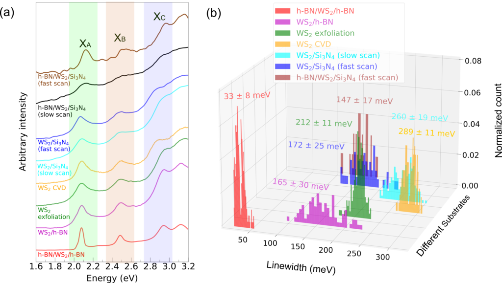
The excitonic states of transition metal dichalcogenide (TMD) monolayers are heavily influenced by their external dielectric environment and depend on the substrate used. In this work, various wide band gap dielectric materials, namely hexagonal boron nitride (h−BN) and amorphous silicon nitride (Si3N4), under different configurations as support or encapsulation material for WS2 monolayers, are investigated to disentangle the factors contributing to inhomogeneous broadening of exciton absorption lines in TMDs using electron energy loss spectroscopy in a scanning transmission electron microscope. In addition, monolayer roughness in each configuration was determined from tilt series of electron diffraction patterns by assessing the broadening of diffraction spots by comparison with simulations. From our experiments, the main factors that play a role in linewidth broadening can be classified, in increasing order of importance, by monolayer roughness, surface cleanliness, and substrate-induced charge trapping. Furthermore, because high-energy electrons are used as a probe, electron-beam-induced damage on bare TMD monolayers is also revealed to be responsible for irreversible linewidth increases. h−BN not only provides clean surfaces of TMD monolayers and minimal charge disorder, but can also protect the TMD from irradiation damage. This work provides a better understanding of the mechanisms by which h−BN remains, to date, the most compatible material for 2D material encapsulation, facilitating the realization of intrinsic material properties to their full potential.
Reference
F. Shao et al., Phys. Rev. Mater. 6, 074005 (2022) DOI:10.1103/PhysRevMaterials.6.074005