In the quest for new materials, one can either explore the collections of a natural sciences museum in order to see what Nature offers, or synthetize them from our ideas about the control of their properties. An important asset of the second strategy is the possibility to prepare artificial materials by stacking layers as thin as a few atoms. In such samples, the interfacial atoms amount to a significant fraction, so that the material properties can be fixed by the internal interfaces. But how do these interfaces look like?

In the case of magnetic materials, interface effects have been studied for more than 40 years, following the development of the necessary technology. One demonstrative example is the interfacial magnetic anisotropy, predicted in 1953 by Louis Néel (physics 1970 Nobel prize) and observed at the beginning of the 80’s. Its effect is to align the magnetic moments in the direction normal to the surface, opposite to the familiar magnetostatic effect following which a compass needle is magnetized along its length, and an iron sheet within its plane. Other interfacial magnetic properties have been found later, fueling the development of magnetic devices that now constitute the so-called spintronics, such as the sensors based on the giant magnetoresistance effect (2007 physics Nobel prize to Albert Fert and Peter Grünberg), and more recently the magnetic random access memories (MRAM) that incorporate non-volatile memory directly inside the electronic components. Another recently observed interfacial magnetic property is the Dzyaloshinskii-Moriya interaction (DMI), which tends to orient neighbouring magnetic moments at right angles, within a plane and in a sense fixed by the DMI type. This directly competes with the major magnetic interaction – called exchange – which aligns these moments. As generally DMI is weak in comparison to exchange, it has taken more than 30 years to evidence it in the samples of spintronics, even if it had been predicted to occur in 1992 by Albert Fert.
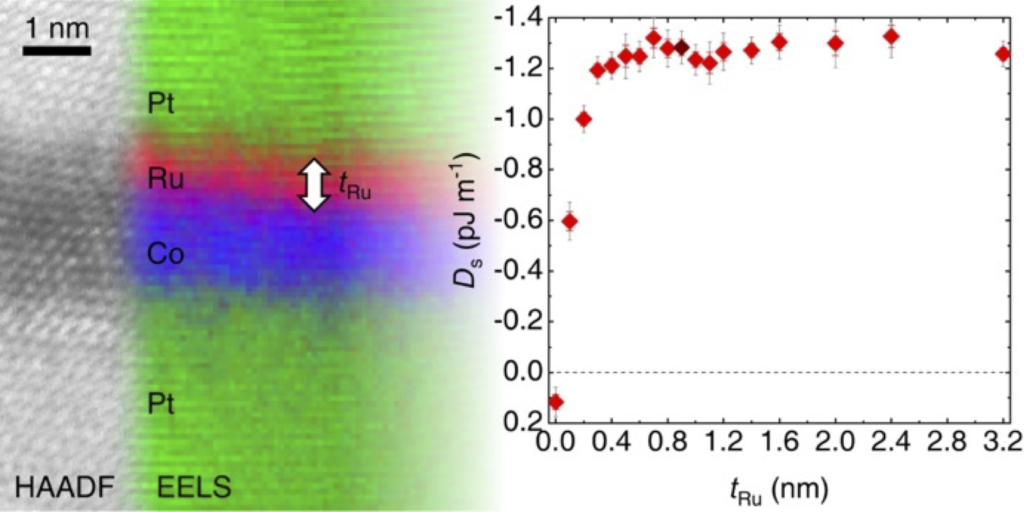
From a structural point of view, as soon as B atoms are deposited on the surface of A atoms, the B/A interface is formed. But from the point of view of electrons, how many atomic layers of B are necessary to form the interface with its specific properties, and what happens if the thickness of the A layer is itself reduced? A team of physicists from Université Paris-Saclay (Unité Mixte de Physique CNRS-Thales, STEM and IDMAG groups of the Laboratoire de Physique des Solides), in collaboration with the the Forschungszentrum Jülich (Peter Grünberg Institut) in Germany has undertaken a multi-technique study, including theory, of the impact of the number of atomic layers on the interfacial DMI as well as exchange. Samples have been elaborated with average thicknesses increasing by 0.1 nm steps (one half the size of a Co atom). The atomic and chemical structure of the samples has been probed by transmission electron microscopy, the chemical information coming from the electrons’ energy losses (see Figure). Magnetic properties have been mainly measured by inelastic light scattering by spin waves (Brillouin light scattering), using a setup recently installed at LPS with the support of Université Paris-Saclay, CNRS, laboratoire d’excellence NanoSaclay and the Ile-de-France region.
The results show that, for layers grown by physical vapor deposition (sputtering), a single atomic plane of ruthenium is sufficient to form the interface with cobalt, whereas two planes of platinum are required. The difference between the two metals is also seen in the structural images. The electronic structure calculations confirm the two different distances, even if they were made for perfect atomic structures, confirming that the observed effect is intrinsic. This work opens perspectives for the synthesis of materials optimized for spintronics.
Reference
Spatial extent of the Dzyaloshinskii-Moriya interaction at metallic interfaces, W. Legrand, Y. Sassi, F. Ajejas, S. Collin, L. Bocher, H. Jia, M. Hoffmann, B. Zimmermann, S. Blügel, N. Reyren, V. Cros , & A. Thiaville Physical Review Materials, 2022, 6, 024408 (editor’s suggestion)
