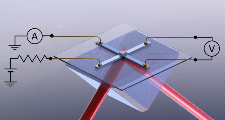
Rectification of an optical signal using an all-metallic electronic device is of fundamental and technological importance for nano-optics. Researchers probed experimentally the microscopic mechanism at the origin of the optical rectification in metal-insulator-metal junctions.
Recent years have seen tremendous progress in plasmonics and nanophotonics with the realization of optical nanoantennas, which can receive and emit radiation at optical frequencies. Optical rectification describes a nonlinear optical process that can be exploited by nanoantennas to convert optical radiation to a DC voltage, acting as a type of detector. However, despite recent experimental efforts in the development of electrically-driven plasmonic sources, the interplay between quantum transport and optics is still under debate.
Researchers from Laboratoire de Physique des Solides used a metallic tunnel junction under infrared illumination (λ = 1550 nm, Figure) to address the microscopic mechanism at the origin of optical rectification, a work recently published in Communications Physics. They compared the photon-assisted current and the current-voltage characteristic of the junction measured on a voltage range much greater than (hc)/(eλ) ≈ 0.825 V. The experimental results do not agree with the theory based on the existence of a non-thermal distribution function corresponding to the exchange of energy quanta between electrons and photons. They demonstrate instead that the illumination power mainly goes into heating and that the rectification results from the tunneling Seebeck effect. These results open new theoretical and experimental investigations to highlight the hot carrier distribution in illuminated metallic thin films.

Reference
Role of optical rectification in photon-assisted tunneling current
P. Février, J. Basset, J. Estève, M. Aprili, J. Gabelli
Communications Physics, 2023, 6, 29
doi: 10.1038/s42005-023-01149-5
Contact
Julien Gabelli
