Contact: Antonio TEJEDA
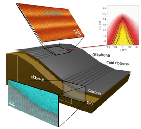
Band gap opening in graphene nanoribbons
We have studied the last-layer topography and beyond by combining scanning tunneling microscopy and transmission electron microscopy. The main body of the ribbons is bordered by regions where the SiC substrate has nanofacets. It is possible to grow a single graphene layer over the nanofacets as well as over the main facet. We have observed by photoemission that the electronic properties of the continuous graphene layer change depending on the region. On top of the nanofacets there are graphene nanoribbons. These nanoribbons are attached to the SiC substrate on their two edges, in a semiconducting region. The graphene between the attached parts is decoupled from the substrate and it exhibits a band gap of more than 500 meV because of the electronic confinement in these small nanoribbons of 1-2 nm width.
Electronic confinement in self-organized surfaces
The growth of self-organized systems can be used to tailor the electronic properties of the substrate. This is possible because surface states are localized in the last atomic layers and are sensitive to modifications in these layers. It is possible to create a self-organized network of islands that induces a periodic modification of the surface potential. In this way, a network of periodic quantum boxes can be settled to study their electronic properties. Co islands can be indeed self-organized on top of a stepped (vicinal) Au surface. The Au surface state is confined by the Co islands and the surface steps. The periodicity of the system allows to use photoemission to measure the band structure and obtain the surface potential.
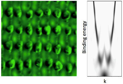
On the left, differential conductance image of self-organized Co islands on a stepped substrate of Au. The intensity in between each four islands shows that the surface state is confined there. On the right, simulation of the photoemission measurements in order to determine the surface potential induced by Co islands.
“Interacting quantum box superlattice by self-organized Co nanodots on Au(788)”. C. Didiot, A. Tejeda, Y. Fagot-Revurat, V. Repain, B. Kierren, S. Rousset, and D. Malterre, Phys. Rev. B 76, 081404(R) (2007).
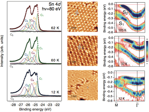
Metal-insulator transition and charge order in Sn/Ge(111)
The search for two dimensional Mott insulators has begun on the 1990s with K/Si(111):B and SiC(0001). In 2006, we have discovered a new metal-insulator transition for 1/3 ML Sn on Ge(111) under 30 K. We have interpreted these observations in terms of a Mott transition.
In Sn/Ge(111), the metallic (3×3) reconstruction that appears around 200 K was considered as the fundamental state. However, our complementary experiments of low energy electron diffraction, angle-resolved photoemission and scanning tunneling microscopy have allowed us to discover two new phases. Below 60 K the system becomes a bad metal while preserving the (3×3) surface symmetry. It is a charge ordered insulating phase. Under 30 K, the surface symmetry changes to (√3 x √3)R30°, where the vertical distortion of Sn atoms in the (3×3) phase is lost. All the Sn atoms are equivalent. Photoemission using synchrotron radiation shows that the structural phase transition, also observed in the core levels, is concomitant to a band gap opening. This experimental observations are compatible with the onset of a Mott insulating phase.
Phase transitions in Sn/Ge(111). Left column, Sn 4d core levels for three temperatures characteristic of each phase. Middle column, STM images showing the charge order in the intermediate phase and the equivalence of all the Sn atoms at the low temperature phase. Right column, electronic structure showing the bad metallicity of the intermediate phase and the large gap at the low temperature phase. Figures from R. Cortés et al., Phys. Rev. B 88, 125113 (2013). Copyright 2013 by the American Physical Society.” http://dx.doi.org/10.1103/PhysRevB.88.125113
Observation of a Mott insulating ground state for Sn/Ge(111) at low temperature R. Cortés, A. Tejeda, J. Lobo, C. Didiot, B. Kierren, D. Malterre, E.G. Michel and A. Mascaraque. Physical Review Letters 96, 126103 (2006). http://dx.doi.org/10.1103/PhysRevLett.96.126103
Highlight in Nature News & Views 441, 295 (2006).
Transition in Sn/Si(111):B by ultrafast collective diffusion
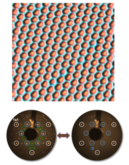
The Sn/Si(111) interface doped with B is a good candidate to look for Mott insulators, as it is hybrid between Sn/Si(111) and K/Si:B interfaces, both prone to exhibit electronic correlation effects. On Sn/Si(111):B we have found an insulating phase at room temperature that exhibits a reversible phase transition at 520 K, giving rise to a different surface symmetry. This phase transition is explained by a the collective fluctuation of Sn surface atoms at the picosecond scale. These fluctuations correspond to Sn tetramers exploring the 24 energy-degenerated configurations as a function of time.
Phase transition in Sn/Si(111):B. On the top, STM image showing the order of the Sn/Si(111):B surface at room temperature. On the bottow, low energy electron diffraction patterns showing the reversible symmetry change at the surface around 520 K. Figure from W. Srour et al., Phys. Rev. Lett. 114, 196101 (2015). Copyright 2015 by the American Physical Society.” http://dx.doi.org/10.1103/PhysRevLett.114.196101