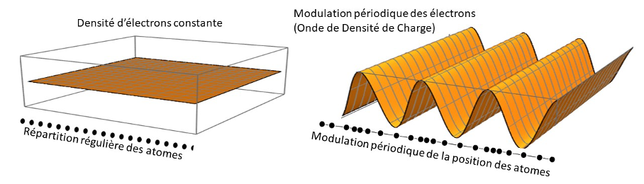
The LUTECE team of LPS team has just observed the shear of a charge density wave under an applied electric current by scanning X-ray diffraction. A charge density wave is a state which appears in some crystals and which corresponds to a periodic modulation of the electrons accompanied by a periodic distortion of the atom lattice. This wave has the ability to slide through the crystal. In the 1980s, J. Friedel and D. Feinberg even predicted that this wave should bend under an applied electric current [1]. This effect had never been observed before, however, because the deformation continuously extends over too great distances. However, this deformation plays a fundamental role since it is at the origin of the nucleation of solitons (point defects) which, once in motion, create a very stable form of electric current.
Finely observing a crystal over great distances with atomic resolution has always been an experimental challenge in condensed matter. Observing the deformation of a charge density wave requires mapping an object with a period of ten angstroms over tens of micrometers, that is over more than 4 orders of magnitude. To do this, the researchers used a focused X-beam produced from the synchrotron source at ESRF in Grenoble and continuously scanned the sample surface with a 300nm beam.
The team were interested in the NbSe3 system which exhibits exceptional transport properties linked to the dynamics of the charge density wave. The sample was submitted to a small dc electric current and prepared so that the current could only be established in its upper part by a cutting line made with FIB (an ion beam cutting technique). The wave deformation in three dimensions could be measured with currents. The phase of the wave was obtained from the diffraction pattern by a so-called phase gradient reconstruction method.
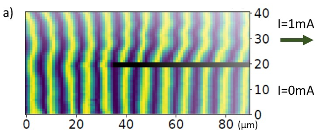
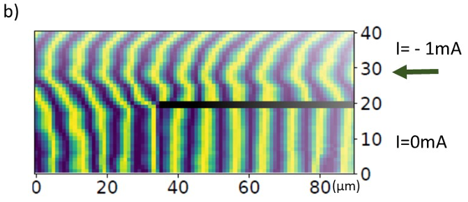
As expected, the wavefronts bend under the applied current. The curvature increases with increasing currents and is reversed when the current is reversed. However, the coherence of the phenomenon and the strain magnitude are surprisingly large, reaching 20 periods in the center of the sample. The deformation remains continuous from one sample edge to the other for more than 40 µm. Despite the presence of many defects, the wave maintains its coherence over more than 20000 times its wavelength. The pinning of the wave in the volume is therefore negligible. Contrary to an established idea, the electronic properties of NbSe3 are mainly driven by surface effects and not the volume, the pinning centers on both edges remaining remarkably stable regardless of the applied currents [2,3].
References
[1] D. Feinberg et J. Friedel, J. Phys. France 49, 485-496 (1988)
[2] Evidence of charge density wave transverse pinning by x-ray microdiffraction
E. Bellec, I. Gonzalez-Vallejo, V. L. R. Jacques, A. A. Sinchenko, A. P. Orlov, P. Monceau, S. J. Leake, and D. Le Bolloc’h
Phys. Rev. B 101, 125122 (2020)
doi: 10.1103/PhysRevB.101.125122
arXiv:1905.03499
PHD E. Bellec (Dec 2019)
[3] The essential role of surface pinning in the dynamics of charge density waves submitted to external dc fields
E. Bellec, V. L. R. Jacques, J. Caillaux, D. Le Bolloc’h
Eur. Phys. J. B 93, 165 (2020)
doi:10.1140/epjb/e2020-10211-6
arXiv:2006.08964